The Xilinx XC9572XL user CPLD means the EB675001DIP often requires very little external logic to implement a large variety of tasks.
The EB675001DIP has the ability to program the user CPLD with an XSVF file from the ABLE command prompt. The Xilinx tools can be used to generate an XSVF programming file of the user CPLD code. The PlayXSVF utility is executed from the ABLE command line which reconfigures the on board JTAG chain and programs the user CPLD without the use of an external JTAG cable. This is documented in the PlayXSVF User Guide.
The user CPLD is connected to the OKI processors external data, address and control lines as shown in Figure 4.7, “Pseudo schematic fragment of EB675001DIP user CPLD”. There are 40 uncommitted CPLD pins available on the expansion headers. The schematic fragment does show all the lines and the CPLD pins they are connected to however the EB675001DIP resources User CPLD section contains some examples and template projects for use with Xilinx webpack software. These examples include a suitable constraints and pin naming file so the signals can be referred to with meaningful symbolic names.
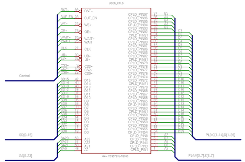
The user CPLD is coupled into the CPU IO XWAIT signal (on CPLD pin 25) which allows I/O cycles to be extended by slow peripherals. The XWAIT is only used by the CPU within the first external chip select region (CS0). The inverted I/O wait request from the Ethernet controller is also brought to the CPLD (pin 20). The designer must ensure the relevant logic is used to combine the nWAIT input and any internal I/O wait requirement to generate a correct XWAIT output. The supplied templates include the VHDL
xwait_o <= '1'
	when nwait_i='0' or user_wait_n='0' else '0'; user_wait_n
	<= '1';
or the schematic fragment
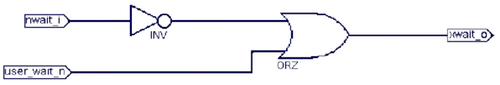
any user design must include this or something very
similar or the module will appear to stop on any IO
access.
The CPLD is intended to be accessed as a memory mapped device using the OKI processors external memory controller. The ML675001 has four external I/O regions these are decoded into 64MB regions at 0xF0000000, 0xF4000000, 0xF8000000 and 0xFC000000. A read or write by the CPU to these regions causes a full external I/O cycle to be performed qualified by the appropriate chip select lines CS0, CS1, CS2 or CS3. The OKI manual contains full information on how to adjust timing cycles and access type as appropriate.
The user CPLD has access to half of the CS0 area and all of CS2 and CS3. The CS0 signal presented to the user CPLD (sometimes referred to as CPLD_ENABLE) has already been decoded by the system CPLD and is active only for the first 32MB of the region, the other 32MB being decoded to the Ethernet controller. The CS0 area is provided, address space 0xF0000000 to 0xF0DFFFFF, because only in this region can the I/O Wait line be used to delay an IO cycle CPLD.
If the user design needs to generate interrupts an interrupt line one of IRQ1, IRQ2 and IRQ3 (on pins A12 A11 A10) should be connected to a CPLD nearby pin (A3 to A7). The IRQ0 should not be used as this is shared with the Ethernet controller and unless specially coded for will prevent correct network operation.
The CLK input is connected to the OKI CPU CKO clock output pin this clock runs at the CPU HCLK frequency which is typically configured to 58.976MHz (7.372MHz baud rate clock with PLL multiplier of 8).
The reset line is the global system reset and should be used to reset any internal state. The signal is active low and is typically held for several ms.
The numerous application notes that accompany the EB675001DIP web resources should give some further ideas to a designer.