The IM2440D20 edge connections are JEDEC standard 200pin SODIMM compatible. The connector is keyed to 2.5V and any suitable SODIMM socket may be used.
These connectors provide all the I/O signals to expand the use of the module. For full details the IM2440D20 Connector and link pinouts document should be consulted, this contains addition information and comments relevant to using this product.
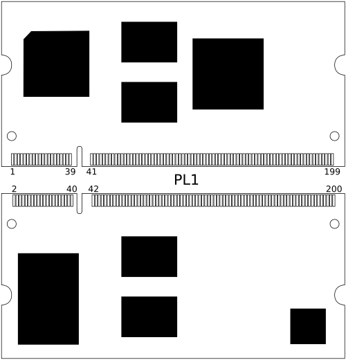
Table 2.1. 200 way edge connector PL1
| Description | Name | Pin | Pin | Name | Description |
|---|---|---|---|---|---|
| Output supply from module | VOUT | 1 | 2 | GND | Ground |
| Inverted read enable | nFRE | 3 | 4 | ALE | NAND address latch enable |
| NAND Inverted write enable | nFWE | 5 | 6 | CLE | NAND Command latch enable |
| Third NAND chip select | nFCE2 | 7 | 8 | R/nB | NAND ready/not busy |
| Data bus bit 0 | D0 | 9 | 10 | D16 | Data bus bit 16 |
| Data bus bit 1 | D1 | 11 | 12 | D17 | Data bus bit 17 |
| Data bus bit 2 | D2 | 13 | 14 | D18 | Data bus bit 18 |
| Data bus bit 3 | D3 | 15 | 16 | D19 | Data bus bit 19 |
| Data bus bit 4 | D4 | 17 | 18 | D20 | Data bus bit 20 |
| Data bus bit 5 | D5 | 19 | 20 | D21 | Data bus bit 21 |
| Data bus bit 6 | D6 | 21 | 22 | D22 | Data bus bit 22 |
| Data bus bit 7 | D7 | 23 | 24 | D23 | Data bus bit 23 |
| Data bus bit 8 | D8 | 25 | 26 | D24 | Data bus bit 24 |
| Data bus bit 9 | D9 | 27 | 28 | D25 | Data bus bit 25 |
| Data bus bit 10 | D10 | 29 | 30 | D26 | Data bus bit 26 |
| Data bus bit 11 | D11 | 31 | 32 | D27 | Data bus bit 27 |
| Data bus bit 12 | D12 | 33 | 34 | D28 | Data bus bit 28 |
| Data bus bit 13 | D13 | 35 | 36 | D29 | Data bus bit 29 |
| Data bus bit 14 | D14 | 37 | 38 | D20 | Data bus bit 20 |
| Data bus bit 15 | D15 | 39 | 40 | D31 | Data bus bit 31 |
| Key | |||||
| Ground | GND | 41 | 42 | GND | Ground |
| First inverted write byte enable | nWBE0 | 43 | 44 | BUF_EN | Buffer enable |
| Second inverted write byte enable | nWBE1 | 45 | 46 | BUF_DIR | Buffer direction |
| Third inverted write byte enable | nWBE2 | 47 | 48 | PWR_EN | Power good output |
| Forth inverted write byte enable | nWBE3 | 49 | 50 | nRESET | Inverted reset output |
| Inverted I/O wait signal | nWAIT | 51 | 52 | nCS1 | First inverted chip select |
| Inverted sixteen bit access select | nIOCS16 | 53 | 54 | nCS2 | Second inverted chip select |
| Inverted read select | nRD | 55 | 56 | nCS3 | Third inverted chip select |
| Inverted write select | nWR | 57 | 58 | nCS4 | Fourth inverted chip select |
| Ground | GND | 59 | 60 | nCS5 | Fifth inverted chip select |
| Address bus bit 0 | A0 | 61 | 62 | A15 | Address bus bit 15 |
| Address bus bit 1 | A1 | 63 | 64 | A16 | Address bus bit 16 |
| Address bus bit 2 | A2 | 65 | 66 | A17 | Address bus bit 17 |
| Address bus bit 3 | A3 | 67 | 68 | A18 | Address bus bit 18 |
| Address bus bit 4 | A4 | 69 | 70 | A19 | Address bus bit 19 |
| Address bus bit 5 | A5 | 71 | 72 | A20 | Address bus bit 20 |
| Address bus bit 6 | A6 | 73 | 74 | A21 | Address bus bit 21 |
| Address bus bit 7 | A7 | 75 | 76 | A22 | Address bus bit 22 |
| Address bus bit 8 | A8 | 77 | 78 | A23 | Address bus bit 23 |
| Address bus bit 9 | A9 | 79 | 80 | A24 | Address bus bit 24 |
| Address bus bit 10 | A10 | 81 | 82 | A25 | Address bus bit 25 |
| Address bus bit 11 | A11 | 83 | 84 | A26 | Address bus bit 26 |
| Address bus bit 12 | A12 | 85 | 86 | TCLK0 | Timer 0 output |
| Address bus bit 13 | A13 | 87 | 88 | TOUT0 | First PWM output |
| Address bus bit 14 | A14 | 89 | 90 | TOUT1 | Second PWM output |
| Ground | GND | 91 | 92 | TOUT2 | Third PWM output |
| First DMA acknowledge | DACK0 | 93 | 94 | TOUT3 | Fourth PWM output |
| First DMA request | DREQ0 | 95 | 96 | DACK1 | Second DMA acknowledge |
| I2S left right select | I2S_LRCLK | 97 | 98 | DREQ1 | Second DMA request |
| I2S clock | I2S_CLK | 99 | 100 | EINT0 | External interrupt 0 |
| I2S command/data select | I2S_CDCLK | 101 | 102 | EINT1 | External interrupt 1 |
| I2S serial data in | I2S_SDI | 103 | 104 | EINT2 | External interrupt 2 |
| I2S serial data out | I2S_SD0 | 105 | 106 | EINT3 | External interrupt 3 |
| SD card clock | SDCLK | 107 | 108 | EINT4 | External interrupt 4 |
| SD card command | SDCMD | 109 | 110 | EINT5 | External interrupt 5 |
| SD card first data line | SDDATA0 | 111 | 112 | EINT6 | External interrupt 6 |
| SD card second data line | SDDATA1 | 113 | 114 | EINT7 | External interrupt 7 |
| SD card third data line | SDDATA2 | 115 | 116 | EINT8 | External interrupt 8 |
| SD card fourth data line | SDDATA3 | 117 | 118 | EINT9 | External interrupt 9 |
| SPI bus master in slave out | SPIMISO | 119 | 120 | EINT10 | External interrupt 10 |
| SPI bus master out slave in | SPIMOSI | 121 | 122 | EINT11 | External interrupt 11 |
| SPI bus clock | SPICLK | 123 | 124 | EINT12 | External interrupt 12 |
| I2C bus clock | SCL | 125 | 126 | EINT13 | External interrupt 13 |
| I2C bus data | SDA | 127 | 128 | EINT14 | External interrupt 14 |
| Ground | GND | 129 | 130 | EINT15 | External interrupt 15 |
| Line end | LEND | 131 | 132 | EINT16 | External interrupt 16 |
| Video clock | VCLK | 133 | 134 | RTS1 | Second serial port request to send |
| Horizontal sync | HS | 135 | 136 | CTS1 | Second serial port clear to send |
| Vertical sync | VS | 137 | 138 | EINT19 | External interrupt 19 |
| Video data enable | DE/VM | 139 | 140 | CTS0 | First serial port clear to send |
| Video data 0 | VD0 | 141 | 142 | RTS0 | First serial port request to send |
| Video data 1 | VD1 | 143 | 144 | TX0 | First serial transmit |
| Video data 2 | VD2 | 145 | 146 | RX0 | First serial receive |
| Video data 3 | VD3 | 147 | 148 | TX1 | Second serial transmit |
| Video data 4 | VD4 | 149 | 150 | RX1 | Second serial receive |
| Video data 5 | VD5 | 151 | 152 | TX2 | Third serial transmit |
| Video data 6 | VD6 | 153 | 154 | RX2 | Third serial receive |
| Video data 7 | VD7 | 155 | 156 | VOUT | Output supply from module |
| Video data 8 | VD8 | 157 | 158 | GND | Ground |
| Video data 9 | VD9 | 159 | 160 | ADC0 | Analog input 0 |
| Video data 10 | VD10 | 161 | 162 | ADC1 | Analog input 1 |
| Video data 11 | VD11 | 163 | 164 | ADC2 | Analog input 2 |
| Video data 12 | VD12 | 165 | 166 | ADC3 | Analog input 3 |
| Video data 13 | VD13 | 167 | 168 | ADC4 | Analog input 4 |
| Video data 14 | VD14 | 169 | 170 | ADC5 | Analog input 5 |
| Video data 15 | VD15 | 171 | 172 | ADC6 | Analog input 6 |
| Video data 16 | VD16 | 173 | 174 | ADC7 | Analog input 7 |
| Video data 17 | VD17 | 175 | 176 | GND | Ground |
| Video data 18 | VD18 | 177 | 178 | DN0 | USB first channel data negative |
| Video data 19 | VD19 | 179 | 180 | DP0 | USB first channel data positive |
| Video data 20 | VD20 | 181 | 182 | DN1 | USB second channel data negative |
| Video data 21 | VD21 | 183 | 184 | DP1 | USB second channel data positive |
| Video data 22 | VD22 | 185 | 186 | nTRST | Inverted tap reset |
| Video data 23 | VD23 | 187 | 188 | TDI | Tap data input |
| Ground | GND | 189 | 190 | TMS | Tap mode select |
| Real time clock supply | VCC_RTC | 191 | 192 | TCK | Tap clock |
| Power supply | VIN | 193 | 194 | TDO | Tap data out |
| Power supply | VIN | 195 | 196 | nRESET | Inverted reset input |
| Power supply | VIN | 197 | 198 | GND | Power ground |
| Power supply | VIN | 199 | 200 | GND | Power ground |